Scaling up nano for sustainable manufacturing
Developed by a team led by Lawrence Berkeley National Laboratory (Berkeley Lab), the new self-assembling nanosheet could significantly extend the shelf life of consumer products. And because the new material is recyclable, it could also enable a sustainable manufacturing approach that keeps single-use packaging and electronics out of landfills.
The team is the first to successfully develop a multipurpose, high-performance barrier material from self-assembling nanosheets. The breakthrough was reported online in the Nov. 8 issue of the journal Nature.
“Our work overcomes a longstanding hurdle in nanoscience – scaling up nanomaterial synthesis into useful materials for manufacturing and commercial applications,” said Ting Xu, the principal investigator who led the study. “It’s really exciting because this has been decades in the making.”
Xu is a faculty senior scientist in Berkeley Lab’s Materials Sciences Division, and professor of chemistry and materials science and engineering at UC Berkeley.
One challenge in harvesting nanoscience to create functional materials is that many small pieces need to come together so that the nanomaterial can grow large enough to be useful. And while stacking nanosheets is one of the simplest ways to grow nanomaterials into a product, “stacking defects” – gaps between the nanosheets – are unavoidable when working with existing nanosheets or nanoplatelets.
“If you visualize building a 3D structure from thin, flat tiles, you'll have layers up the height of the structure, but you'll also have gaps throughout each layer wherever two tiles meet,” said first author Emma Vargo, a former graduate student researcher in the Xu group and now a postdoctoral scholar in Berkeley Lab’s Materials Sciences Division. “It’s tempting to reduce the number of gaps by making the tiles bigger, but they become harder to work with,” Vargo said.
The new nanosheet material overcomes the problem of stacking defects by skipping the serial stacked sheet approach altogether. Instead, the team mixed blends of materials that are known to self-assemble into small particles with alternating layers of the component materials, suspended in a solvent. To design the system, the researchers used complex blends of nanoparticles, small molecules, and block copolymer-based supramolecules, all of which are commercially available.
Experiments at Oak Ridge National Laboratory’s Spallation Neutron Source helped the researchers understand the early, coarse stages of the blends’ self-assembly. As the solvent evaporates, the small particles coalesce and spontaneously organize, coarsely templating layers, and then solidify into dense nanosheets. In this way, the ordered layers form simultaneously rather than being stacked one by one in a serial process. The small pieces only need to move short distances to get organized and close gaps, avoiding the problems of moving larger “tiles” and the inevitable gaps between them.
From a previous study led by Xu, the researchers knew that combining nanocomposite blends containing multiple “building blocks” of various sizes and chemistries, including complex polymers and nanoparticles, would not only adapt to impurities but also unlock a system’s entropy, the inherent disorder in mixtures of materials that Xu’s group harnessed to distribute the material’s building blocks.
The new study builds on this earlier work. The researchers predicted that the complex blend used for the current study would have two ideal properties: In addition to having high entropy to drive the self-assembly of a stack of hundreds of nanosheets formed simultaneously, they also expected that the new nanosheet system would be minimally affected by different surface chemistries. This, they reasoned, would allow the same blend to form a protective barrier on a variety of surfaces, such as the glass screen of an electronic device, or a polyester mask.
Demonstrating a new 2D nanosheet’s ease of self-assembly and high performance
To test the performance of the material as a barrier coating in several different applications, the researchers enlisted the help of some of the nation’s best research facilities.
During experiments at Argonne National Laboratory’s Advanced Photon Source, the researchers mapped out how each component comes together, and quantified their mobilities and the manner in which each component moves around to grow a functional material.
Based on these quantitative studies, the researchers fabricated barrier coatings by applying a dilute solution of polymers, organic small molecules, and nanoparticles to various substrates – a Teflon beaker and membrane, polyester film, thick and thin silicon films, glass, and even a prototype of a microelectronic device – and then controlling the rate of film formation.
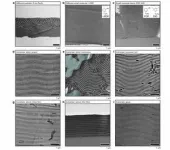
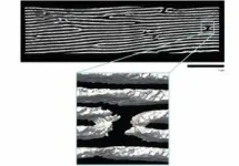
Transmission electron microscope experiments at Berkeley Lab’s Molecular Foundry show that by the time the solvent had evaporated, a highly ordered layered structure of more than 200 stacked nanosheets with very low defect density had self-assembled on the substrates. The researchers also succeeded in making each nanosheet 100 nanometers thick with few holes and gaps, which makes the material particularly effective at preventing the passage of water vapor, volatile organic compounds, and electrons, Vargo said.
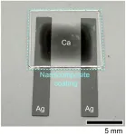
Other experiments at the Molecular Foundry showed that the material has great potential as a dielectric, an insulating “electron barrier” material commonly used in capacitors for energy storage and computing applications.
In collaboration with researchers in Berkeley Lab’s Energy Technologies Area, Xu and team demonstrated that when the material is used to coat porous Teflon membranes (a common material used to make protective face masks), it is highly effective in filtering out volatile organic compounds that can compromise indoor air quality.
And in a final experiment in the Xu lab, the researchers showed that the material can be redissolved and recast to produce a fresh barrier coating.
Now that they’ve successfully demonstrated how to easily synthesize a versatile functional material for various industrial applications from a single nanomaterial, the researchers plan to finetune the material’s recyclability and add color tunability (it currently comes in blue) to its repertoire.
Other authors on the paper are Le Ma, He Li, Qingteng Zhang, Junpyo Kwon, Katherine M. Evans, Xiaochen Tang, Victoria L. Tovmasyan, Jasmine Jan, Ana C. Arias, Hugo Destaillats, Ivan Kuzmenko, Jan Ilavsky, Wei-Ren Chen, William Heller, Robert O. Ritchie, and Yi Liu.
The technology is available for licensing or collaborative research through Berkeley Lab’s Intellectual Property Office. Contact ipo@lbl.gov for more information.
The Molecular Foundry is a DOE Office of Science user facility at Berkeley Lab.
The Advanced Photon Source is a DOE Office of Science user facility at Argonne National Laboratory.
The Spallation Neutron Source is a DOE Office of Science user facility at Oak Ridge National Laboratory.
The work was supported by DOE’s Office of Science and Berkeley Lab’s Laboratory Directed Research and Development (LDRD) program. Additional funding was provided by the Department of Defense, the National Science Foundation, and the Defense Threat Reduction Agency.
###
Lawrence Berkeley National Laboratory (Berkeley Lab) is committed to delivering solutions for humankind through research in clean energy, a healthy planet, and discovery science. Founded in 1931 on the belief that the biggest problems are best addressed by teams, Berkeley Lab and its scientists have been recognized with 16 Nobel Prizes. Researchers from around the world rely on the Lab’s world-class scientific facilities for their own pioneering research. Berkeley Lab is a multiprogram national laboratory managed by the University of California for the U.S. Department of Energy’s Office of Science.
DOE’s Office of Science is the single largest supporter of basic research in the physical sciences in the United States, and is working to address some of the most pressing challenges of our time. For more information, please visit energy.gov/science.
END


