Control of light–matter interactions in two-dimensional materials with nanoparticle-on-mirror structures
A new publication from Opto-Electronic Sciences; DOI 10.29026/oes.2024.230051 , discusses control of light–matter interactions in two-dimensional materials with nanoparticle-on-mirror structures.
With the rapid development of high bit-rate wireless services driven by mobile internet, AI computing, high-definition videos, virtual reality/augmented reality (VAR) applications, and so on, the demand for wireless data rates has grown explosively in the past decades1, 2. Supporting such fast data rate at tens of Gbit/s pushes the carrier frequency to the THz (0.1-10 THz) domain in 6G to accommodate the bandwidth-hungry wireless services. Optoelectronics based THz technology have lots of advantages, and photodiodes (PDs) serve as a key component of photonic transmitter to realize optical-to-electrical conversion. In particular, uni-traveling-carrier photodiodes (UTC-PDs) have been developed to simultaneously achieve both ultrawide bandwidth and high output power. At the same time, module packaging of high-speed PDs is important for their applications in millimeter wave or THz wireless communications. This paper presents a wide-bandwidth back-illuminated modified uni-traveling-carrier photodiode (MUTC-PD) packaged with standard WR-5 rectangular waveguide for high-speed wireless communications. The over 80 GHz bandwidth of the PD module at G-band promises other broadband applications, such as THz spectroscopy and imaging. Furthermore, with the high saturated output power, the PD module has the potential to achieve high-performance 6G THz wireless communication.
In view of the trade-off between the large bandwidth and high saturation power performance of the PD chip, and the domestic blank of high-speed photomixer modules. The article studies from high-performance PD chip, low-loss THz thin film circuit to high-speed photomixer module. The epitaxial structure of the MUTC-PD illustrated in Fig. 1(a) supports high-speed carrier transport. At the same time, high-speed transport of electrons can also alleviate the space charge effect, and thus break the trade-off between large bandwidth and high saturation. As shown in Fig. 1(b), inductive electrodes are used to compensate the chip capacitance to expand the bandwidth and comprehensively improve the chip's bandwidth and output power performance. The article uses a three-mesa device manufacturing process to improve yield and consistency. The 3D schematic of the 4-μm-diameter PD is illustrated in Fig. 1(c), which adopts a triple-mesa structure for improved fabrication yield and consistency. A combination of dry-etching and wet-etching process is employed to define the mesas. Scanning electron microscope (SEM) image of the fabricated device is shown in Fig. 1(d). The frequency response of the fabricated 4-μm-diameter MUTC-PD at G-band are measured with a two-laser heterodyne system. The frequency responses under different photocurrents with a fixed reverse bias of 2 V are plotted in Fig. 1(e). The PD exhibits ultra-flat frequency responses over the entire G-band under various photocurrents.
To package the high-speed PD chip into a compact module with waveguide output, it is essential to realize smooth transition from the CPW electrodes on the PD to the waveguide port. In addition, a bias-tee is also required to provide dc bias to the module. A back-to-back probe package and bias-tee are fabricated to verify the performance, which both exhibit low-loss transmission.
The fully packaged MUTC-PD with standard WR-5 output is shown in Fig. 2(a). The frequency responses tested under a reverse bias of 2 V are plotted in Fig. 2(b). The PD module exhibits a flat frequency response with a fluctuation within ±2.75 dB over 140-220 GHz under various photocurrents. The frequency-dependent saturation characteristics of the packaged PD is shown in Fig. 4(c). The saturation photocurrent under 140, 150, and 160 GHz is 8.6, 8.3, 7.7 mA, corresponding to a saturation power of -7.8, -8.3, and -8.9 dBm, respectively. The proposed MUTC-PD module with rectangular waveguide output shows high saturation power at high frequencies.
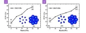
The packaged PD module has been successfully employed for photonics-assisted THz wireless communication. As shown in Fig. 3, transmission rates of 75 and 90 Gbps over 1-m free space are demonstrated at 150.5 and 210.5 GHz carrier frequencies, respectively. The over 80 GHz bandwidth of the PD module at G-band promises other broadband applications, such as THz spectroscopy and imaging. Furthermore, with the high saturated output power, the PD module has the potential to achieve high-performance 6G THz wireless communication. The research of the THz photoelectric integrated device is of great scientific significance and wide application prospect for the next generation mobile communication technology (6G).
Keywords: modified uni-traveling-carrier photodiode / integrated bias-tee / E-plane probe / flat frequency response / high saturation power / WR-5 output / THz wireless communications
# # # # # #
The Integrated Optoelectronics Laboratory of the Tsinghua University research team is led by Academician/Professor Luo Yi. The integrated optoelectronics laboratory supported by the research team was established in 1987, and passed acceptance, officially operated and opened to the public in January 1991. After more than 30 years of construction, it has grown into one of the main research bases engaged in semiconductor optoelectronic materials and devices and their application technology in optical fiber communication and network, with 600 square meters of ultra-clean laboratory, which can independently conduct the whole chain technology research and development of material epitaxy, chip process, module packaging, evaluation and testing. The laboratory has made outstanding achievements in many important research fields, produced a certain international influence, and trained a large number of research talents for research units and the business community. At present, the laboratory has 1 academician of the Chinese Academy of Engineering, 3 professors, 4 associate professors, 1 assistant researcher, 1 post-doctoral student, and more than 40 candidates for doctoral and master’s degrees. At present, it undertakes national key research and development projects, National Natural Science Foundation and other projects. With the joint efforts of teachers and students, the laboratory has won a number of honors and awards, including 3 second prizes of national technological invention, 1 second prizes of National scientific and technological progress, and several provincial and ministerial awards.
The Intelligent photonic communication research group led by President Chi Nan is based on the Key Laboratory of Electromagnetic Wave Information Science of the Ministry of Education of Fudan University headed by Academician Jin Yaqiu. The research group has long been engaged in research in the field of spatial information transmission technology. In recent years, the research group has carried out in-depth research in the fields of high-speed space communication in new spectrum such as visible light, infrared, millimeter wave and terahertz, intelligent photon signal processing and sensing communication integration, and published a series of high-level papers more than 300, which has produced a greater academic influence. At present, the laboratory has 1 winner of the National Outstanding Youth Fund, 1 overseas high-level Young Talent title, 2 Shanghai High-level Talent title and other outstanding scientific researchers and more than 40 postgraduate students. The research group has undertaken more than 20 national, provincial and ministerial level projects such as a number of key research and development programs of the Ministry of Science and Technology and key projects of the Natural Science Foundation, and the results have been applied to many industries, and have produced significant social and economic benefits.
# # # # # #
Opto-Electronic Science (OES) is a peer-reviewed, open access, interdisciplinary and international journal published by The Institute of Optics and Electronics, Chinese Academy of Sciences as a sister journal of Opto-Electronic Advances (OEA, IF=15.3). OES is dedicated to providing a professional platform to promote academic exchange and accelerate innovation. OES publishes articles, reviews, and letters of the fundamental breakthroughs in basic science of optics and optoelectronics.
# # # # # #
More information: https://www.oejournal.org/oes
Editorial Board: https://www.oejournal.org/oes/editorialboard/list
OES is available on OE journals (https://www.oejournal.org/oes/archive)
Submission of OES may be made using ScholarOne (https://mc03.manuscriptcentral.com/oes)
CN 51-1800/O4
ISSN 2097-0382
Contact Us: oes@ioe.ac.cn
Twitter: @OptoElectronAdv (https://twitter.com/OptoElectronAdv?lang=en)
WeChat: OE_Journal
# # # # # #
Tian YX, Dong BY, Li YX et al. Photonics-assisted THz wireless communication enabled by wide-bandwidth packaged back-illuminated modified uni-traveling-carrier photodiode. Opto-Electron Sci 3, 230051 (2024). doi: 10.29026/oes.2024.230051
END


