Multi-functional and highly reconfigurable monolithic signal processing system
A new publication from Opto-Electronic Sciences; DOI 10.29026/oes.2024.240012, discusses a multi-functional and highly reconfigurable monolithic signal processing system.
Photonic signal processing offers a versatile and promising toolkit for contemporary scenarios ranging from digital optical communication to analog microwave operation. Compared to its electronic counterpart, it eliminates inherent bandwidth limitations and meanwhile exhibits the potential to provide unparalleled scalability and flexibility, particularly through integrated photonics. Very recently, researchers have put a lot of effort into its integrated form, and to promote the signal processing system in Size, Weight, Power and Cost (SWaP-C). However, by far the on-chip solutions for optical signal processing are often tailored to specific tasks, which lacks versatility across diverse applications. Therefore, developing a chip-level architecture with high versatility and competitive performance remains elusive.
To fully capitalize on the advantages of integrated photonics, a signal processing unit should compromise the following characteristics: Firstly, the chip ought to possess signal loading capabilities, applicable in both analog and digital formats, typically relying on an E/O modulator (array). Secondly, the system should support both coherent and incoherent signal processing. This means processing based on either the principles of spectrum interference or digital signal processing, often through the direct accumulation of orthogonal components like frequency or mode. Moreover, the architecture needs to be as compact as possible to maximize performance per unit area. This includes metrics such as data throughput and processing density, which largely depend on the efficient arrangement of various functional units.
This section should explain the strategies, results, importance and contribution of your work in a broader context in the third person. In terms of words and expression, please consider how to attract both specialist and non-specialist scientific audience.
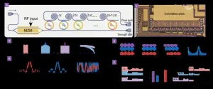
The authors of this article propose a multi-functional and highly reconfigurable monolithic signal processing system and conduct comprehensive and thorough analyses at the levels of device, system, and application. The streamlined chip-level signal processing architecture integrates different active and passive building blocks in silicon-on-insulator (SOI) platform with a compact and efficient manner. Specifically, the system is composed of a high-speed silicon modulator, cascaded microring resonators and delay lines, which showcases multidimensional optical operating abilities including signal loading, wavelength selection, amplitude adjustment, and time delay. The system structure and working principles are shown in Figure 1.
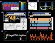
The researchers also conducted in-depth characterization and analysis at the device and system levels, verifying the reliability of the integrated devices, discussing the optimization potential of the architecture, and demonstrating its performance in critical information processing operations. These operations include high-precision weight loading and high-speed information summation, as shown in Figure 2.
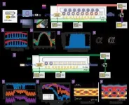
Accompanied by appropriate configuring schemes, the photonic circuitry supports loading and processing both analog and digital signals simultaneously. Three distinct tasks are facilitated with one single chip across several mainstream fields, spanning optical computing, microwave photonics, and optical communications. For microwave processing, it functions as a digital spectrum filter with high main-to-sidelobe suppression ratio and tunable bandwidth. In optical computing, this processing chip can accelerate matrix calculation in image processing, offering high-speed and high-precision operations. In data transmission, it acts as a signal equalizer for bandwidth extension via frequency interference management.
Such system imparts tunability and versatility and works in a mode having both the excellent specialized performance characteristic of the application-specific photonic integrated circuits (ASPICs) architecture and the flexible reconfigurability of the Field Programmable Photonic Gate Arrays (FPPGA) architecture. Boasting high universality and a compact form factor, the proposed architecture is poised to be instrumental for next-generation functional fusion systems.
Keywords: silicon photonics / multifunctional signal process / microwave photonics / optical computing / optical communication equalization
# # # # # #
Wang Xingjun is a Boya Distinguished Professor at Peking University, a doctoral supervisor, and Vice Dean of the School of Electronics. He is also a member of the Discipline Review Group of the State Council, a Changjiang Distinguished Professor appointed by the Ministry of Education, an Optica Fellow, and a Fellow of the Chinese Society for Optical Engineering. Additionally, he serves as the Deputy Director of the State Key Laboratory of Advanced Optical Communication Systems & Networks, the Chief of the National Key R&D Program of China, and the Leader of both the NSFC Key Program and Major Instrument Program.
Wang's team is dedicated to the research and development of large-scale integrated chips and systems based on photonic and electronic devices. They have made significant advancements in silicon-based optoelectronic integrated chips and their applications in optical communication, optical sensing, microwave photonics, and optical computing. Over the past five years, Wang has published more than 60 papers as the first or corresponding author in prestigious journals such as Nature, Nature Photonics, Light: Science & Applications, and Nature Communications. He has also presented over 30 papers at top academic conferences like OFC and CLEO, holds more than 40 authorized invention patents, and has received over 50 invitations to speak at international conferences including OFC, CLEO, OECC, and ACP.
Wang's representative achievements have been recognized with numerous honors, including selection for the China Top Ten Science and Technology Innovation Awards, China Top Ten Developments in Optics, China Top Ten Science and Technology Advances in Information and Communication, Top 10 Social Impact Events in China's Optical Industry (Light 10), and China Top Ten Advances in Chip Science.
Website: https://pcis.pku.edu.cn
# # # # # #
Opto-Electronic Science (OES) is a peer-reviewed, open access, interdisciplinary and international journal published by The Institute of Optics and Electronics, Chinese Academy of Sciences as a sister journal of Opto-Electronic Advances (OEA, IF=15.3). OES is dedicated to providing a professional platform to promote academic exchange and accelerate innovation. OES publishes articles, reviews, and letters of the fundamental breakthroughs in basic science of optics and optoelectronics.
# # # # # #
More information: https://www.oejournal.org/oes
Editorial Board: https://www.oejournal.org/oes/editorialboard/list
OES is available on OE journals (https://www.oejournal.org/oes/archive)
Submission of OES may be made using ScholarOne (https://mc03.manuscriptcentral.com/oes)
CN 51-1800/O4
ISSN 2097-0382
Contact Us: oes@ioe.ac.cn
Twitter: @OptoElectronAdv (https://twitter.com/OptoElectronAdv?lang=en)
WeChat: OE_Journal
# # # # # #
Wu YC, Yang QP, Shen BT et al. Multifunctional mixed analog/digital signal processor based on integrated photonics. Opto-Electron Sci 3, 240012 (2024). doi: 10.29026/oes.2024.240012
END


