Silver oxide nanoclusters shrink a perovskite barrier from 250 nm to 25 nm - unlocking quantum tunneling
California NanoSystems Institute, UCLA
Perovskite semiconductors can do remarkable things in the laboratory. They convert sunlight to electricity with efficiencies rivaling silicon. They detect light across a broad spectrum. They can be manufactured from solution at low temperatures, promising cheap, large-area electronics. But there has always been a catch at the point where metal meets perovskite.
In conventional semiconductors like silicon or gallium arsenide, engineers solved the metal-semiconductor contact problem decades ago through impurity doping - deliberately introducing atoms that flood the interface with charge carriers, allowing current to flow freely. Perovskites resist this approach. They are soft, chemically sensitive crystals that degrade when subjected to the aggressive doping techniques that work for harder materials. The result is a bottleneck: current struggles to enter the semiconductor from the electrode, wasting energy and limiting device speed.
A team at UCLA, led by Xiangfeng Duan, has now found a way around this impasse. Their method, published in Nature Materials, does not try to dope the bulk material at all. Instead, it engineers a vanishingly thin region directly beneath the metal contact - just 25 nanometers deep - where silver oxide nanoclusters pull electrons away from the perovskite and create a locally doped zone. The effect is dramatic: current that previously had to climb over a tall energy barrier can now tunnel straight through it.
The old doorway versus the new one
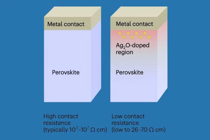
To understand why this matters, picture the metal-perovskite interface as a doorway. In a standard perovskite device, that doorway is blocked by a depletion region roughly 250 nanometers wide - a zone where charge carriers have been swept away, leaving an insulating gap. Current must gather enough thermal energy to leap over this barrier, a process called thermionic emission. It works, but it is inefficient, requiring higher voltages and generating waste heat.
Duan's team shrank the blocked region by a factor of ten. At 25 nanometers, quantum mechanics takes over. Electrons no longer need to jump the barrier; they can pass through it via Fowler-Nordheim tunneling, a phenomenon in which particles traverse an energy wall that classical physics says should stop them. The thinner the wall, the higher the probability of tunneling. At 25 nanometers, the probability becomes high enough to carry practical amounts of current.
The difference between 250 and 25 nanometers is not just quantitative. It represents a shift from one physical regime to another - from classical charge transport to quantum mechanical transport. That shift brings lower contact resistance, lower operating voltages, and faster switching.
How silver oxide clusters form at the interface
The fabrication process involves three steps, each chosen to avoid damaging the perovskite crystal. First, the researchers placed a metal electrode onto the perovskite surface using van der Waals lamination - essentially laying the metal down gently rather than depositing it with high-energy techniques that could disrupt the crystal lattice. This preserves the integrity of the semiconductor surface.
Second, they applied mild thermal annealing, allowing trace amounts of silver from the electrode to diffuse into the top few nanometers of the perovskite. The temperatures involved are modest enough to avoid decomposing the material.
Third, they exposed the interface to ultraviolet light, which converted the diffused silver atoms into silver oxide nanoclusters. These clusters act as electron acceptors: they grab electrons from nearby perovskite molecules, leaving behind positively charged holes. The result is a thin, locally p-doped region directly beneath the contact.
The beauty of the approach is that doping occurs only where it is needed - at the contact interface - and is induced by the contact itself. The bulk of the perovskite remains untouched, preserving its electronic properties for whatever the device is designed to do.
Measuring the tunneling transition
The researchers confirmed the shift from thermionic emission to tunneling through detailed electrical measurements. In devices with conventional contacts, current-voltage curves follow the exponential shape characteristic of thermal activation. In devices with the silver oxide interface, the curves show the distinctive signatures of Fowler-Nordheim tunneling: current increases more steeply with voltage and shows less temperature dependence.
The contact resistance dropped substantially, and the devices operated efficiently at lower voltages. These are exactly the characteristics needed for practical transistors, photodetectors, and other electronic components.
What perovskite electronics still cannot do
This work is a laboratory proof of concept, not a finished technology. The devices were fabricated and tested under controlled conditions, and their long-term stability - always a concern with perovskites - has not been established over the months or years that commercial electronics demand. Perovskites are notorious for degrading when exposed to moisture, heat, and sustained illumination, and it remains unclear whether the silver oxide interface layer will hold up under those stresses.
Scaling the van der Waals lamination process to manufacturing volumes presents its own challenges. Gently placing electrodes on individual devices works in a research lab but is far removed from the high-throughput deposition methods used in semiconductor fabrication.
The study also focused on a specific perovskite composition and a silver-based electrode. Whether the same approach generalizes to the many other perovskite formulations and metal contacts under investigation across the field is an open question. Different perovskite compositions may respond differently to silver diffusion and UV exposure.
A design principle beyond perovskites
Despite these caveats, the concept of contact-induced self-doping - using the electrode itself to create a doped region at the interface - could influence how engineers approach contact design in other emerging semiconductors. Organic semiconductors, two-dimensional materials like molybdenum disulfide, and other solution-processed semiconductors face similar contact resistance challenges. A strategy that localizes doping to the interface without disrupting the bulk material has broad appeal.
For perovskites specifically, the work addresses what many in the field regard as the single largest obstacle to electronic applications beyond solar cells. Perovskite solar cells, where the contact requirements are less demanding, have already reached commercial production. But transistors, logic circuits, and high-speed photodetectors need efficient, low-resistance contacts that perovskites have not previously been able to provide.
The distance from a laboratory demonstration to a commercial perovskite transistor remains long. But the physics now works in a way it did not before. When quantum tunneling replaces thermal hopping at a semiconductor contact, the rules of the game change - and the design space for perovskite electronics expands considerably.