Hafnium oxide memristor draws a millionth the current of conventional devices
University of Cambridge
Conventional AI chips move data constantly between memory and processor, burning electricity at every step. The human brain does the same job — storing and computing — in a single location, on roughly 20 watts. That gap between silicon and synapse is the problem neuromorphic computing aims to close, and the component at its center is the memristor: a resistive device that remembers its state the way a synapse remembers a signal's strength.
The trouble is, most memristors work by growing and rupturing tiny conductive filaments inside a metal oxide. The filaments are erratic. They form in slightly different places each time, demand high voltages, and produce switching behavior that varies from device to device and cycle to cycle. Building a reliable chip from billions of unpredictable switches has proven deeply frustrating.
A different switching mechanism entirely
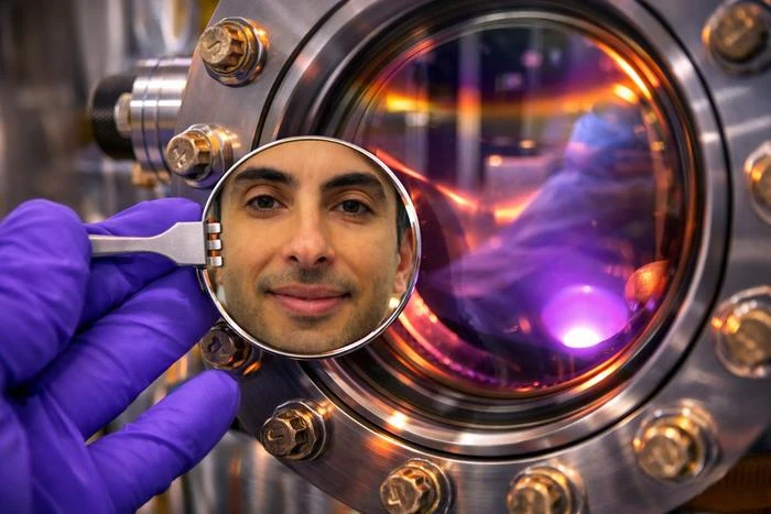
A team led by Dr. Babak Bakhit at the University of Cambridge took a different route. Rather than trying to tame filaments, they eliminated them. By doping hafnium oxide with strontium and titanium and growing the film in a two-step deposition process — adding oxygen only after the first layer — they created a thin-film structure containing internal p-n junctions, tiny electronic gates where two differently doped layers meet.
In this design, resistance changes not because a filament grows or breaks but because the energy barrier at the junction shifts up or down. The switching is smooth, continuous, and — critically — uniform. The same device produces the same response cycle after cycle. Different devices on the same wafer produce the same response as each other.
The results, published in Science Advances, are striking. The junction-based memristors achieved switching currents roughly a million times lower than those of conventional oxide-based devices. They produced hundreds of distinct, stable conductance levels — a key requirement for analog in-memory computing, where information is stored as a gradient of resistance rather than a binary on-off state.
Learning rules, encoded in hardware
Beyond raw efficiency, the devices reproduced biological learning behaviors. In laboratory tests, they demonstrated spike-timing dependent plasticity (STDP), the mechanism neurons use to strengthen or weaken connections based on the precise timing of incoming signals. When two signals arrive close together, the connection strengthens; when the gap widens, it weakens. This is the foundational rule behind how brains learn from experience, and replicating it in hardware means the device can adapt, not just store.
The memristors also survived tens of thousands of switching cycles and retained their programmed states for approximately one day — long enough to demonstrate stability, though well short of the years-long retention commercial memory would require.
Three years of failed experiments
Bakhit, a materials physicist affiliated with Cambridge's departments of Materials Science and Engineering, described the path to the result as anything but smooth. The project consumed nearly three years of unsuccessful fabrication attempts before a late-2025 experiment — adjusting when oxygen was introduced during film growth — produced the first clean switching data.
That kind of timeline is common in materials science, where the difference between a useful device and a useless one can hinge on deposition temperatures, atmospheric composition, or the sequence in which layers are grown. The Cambridge team's two-step approach — growing the base layer without oxygen, then introducing it for the second layer — created the junction structure that makes the whole device work. Without that sequence, the p-n junction does not form, and the film reverts to conventional filamentary behavior.
The 700-degree problem
The most significant obstacle to practical deployment is temperature. The current fabrication process requires approximately 700 degrees Celsius — substantially above what standard semiconductor manufacturing lines can tolerate. CMOS-compatible processes typically cap out around 400 to 450 degrees Celsius. Until the team can bring the thermal budget down, the memristors cannot be integrated onto conventional chips alongside transistors and other components.
Bakhit acknowledged this directly. The temperature constraint is the primary challenge, and the group is actively working on lower-temperature deposition methods. But there is no guarantee the junction structure will form properly at reduced temperatures, and the material properties that make the device work — the precise doping profiles, the crystallinity of the hafnium oxide, the sharpness of the interface — may all be temperature-dependent in ways that are not yet fully understood.
Retention time is another open question. One day of state retention suffices for certain neuromorphic computing paradigms — edge inference, for example, where the network is periodically refreshed — but falls short of non-volatile memory applications. Whether longer retention can be engineered without sacrificing the low switching currents and multi-level stability remains to be demonstrated.
What a million-fold reduction actually buys
The energy arithmetic is straightforward. If a neuromorphic chip contains millions or billions of memristors, each firing thousands of times per second, even modest per-device savings compound into massive system-level reductions. A million-fold drop in switching current — assuming voltage scales proportionally or remains constant — translates to a dramatic cut in power consumption.
Estimates in the neuromorphic computing field suggest that brain-inspired architectures could reduce AI energy use by as much as 70 percent compared to conventional von Neumann designs. Whether that figure holds in practice depends on system-level engineering far beyond any single device, but the Cambridge memristors represent one of the lowest-current oxide switching devices reported to date.
The implications extend beyond AI. Low-power, multi-state resistive devices have potential applications in edge computing, sensor networks, and any domain where energy budgets are tight and adaptability matters — prosthetics, implantable medical devices, autonomous systems operating far from a power grid.
From lab curiosity to chip-scale integration
Cambridge Enterprise, the university's commercialization arm, has filed a patent application on the technology. But a patent is a long way from a product. The fabrication temperature must come down. Retention must go up. The devices must be demonstrated at scale — not one or a handful, but arrays of thousands operating coherently. And the system architecture around them — the readout circuits, the training algorithms, the packaging — must be designed to exploit their unique properties.
Still, the fundamental advance here is real: a memristor that switches by a different physical mechanism, one that is inherently more uniform and draws far less current. Whether this particular material system reaches manufacturing or serves primarily as a proof of concept for junction-based switching, it reframes what is possible in oxide memristor design.
The research was supported by the Swedish Research Council, the Royal Academy of Engineering, the Royal Society, and UK Research and Innovation.