Eco-friendly device developed at UL, Ireland detects real-time pipe damage
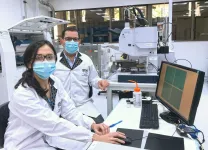
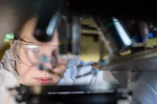
A researcher at University of Limerick has developed a low-cost, environmentally friendly sensor that can detect damage in pipelines and could save water as a result.
The damage detection sensor uses highly sensitive, eco-friendly crystals that generate an electrical signal in response to a leak.
It is the first validation of these biological crystals for real world applications, according to Dr Sarah Guerin, a postdoctoral researcher at the Department of Physics and the Bernal Institute in UL, who has been developing amino acid crystal devices since 2017.
An Irish research collaboration between the Bernal Institute at UL and the Dynamical Systems and Risk Laboratory in University College Dublin has validated ...